Тут описан непосредственно монтаж элементов и их перечень, то есть аппаратная часть чиповки P28. Методика прочтения оригинальной прошивки в отдельной статье. Чиповка P08 и P30 описана в отдельной статье, но технологически процедура похожа. Итак, вся работа по чиповке P28 OBD1 Honda Civic складывается в простых монтажных операциях, а именно:
- Закупка деталей для чиповки OBD1 P28, максимум 300р. ($10)
- Очистка платы от лака с обеих сторон
- Очистка отверстий на плате для посадки деталей
- Запайка новых деталей
- Прошивка чипа памяти параллельным программатором
Инструменты и элементы для пайки, список
Для устанавливания чипов внешней памяти, куда будет закачана модифицированная прошивка, вам понадобятся следующие компоненты, можно найти в электронном магазине типа ChipDip:
- Растворитель лаков, обработайте им поверхность платы с двух сторон, чтобы убрать защитный слой лака
- Мощный паяльник, более 50Вт с узким жалом для работы с платой P28 OBD1
- Отсос припоя или оплетка для снятия припоя
- Припой с флюсом
- Спирт для очищения P28 от флюса после пайки
- Мульти-тестер, для прозвонки контактов
- Скрепка или другая проволока, диаметром чуть менее чем отверстия на плате ECU
- Конденсатор 104, 100 n (нанофарад), 0.1 uF (микрофарад). Посадочное место на плате C51, полярности нет
- Конденсатор 104, 100 n (нанофарад), 0.1 uF (микрофарад). Посадочное место на плате C52, полярности нет
- Резистор 1 кОм (1000 Ом). Посадочное место на плате R54
- Посадочное место J1, если перемычки нет, то используется память внутренняя, при наличии перемычки (J1 на плате), используется память внешняя — вашего чипа
- Чип серии 74HC373 в DIP-корпус. Я использовал MC74HC373N или MM74HC373N, 20 ножек. Нужен для использования прошивки с внешнего чипа памяти
- Чип серии 29C256 в DIP-корпус. Я использовал ATMEL AT29C256 12PC, 28 ножек.
- Многоразовая память (EEPROM), нужен для прошивки вашего мотора
- Чип серии 27C512 DIP-корпус. Я использовал WinBond W27C512, 28 ножек.
- Одноразовая (PROM), нужен для чтения вашей оригинальной, или другой прошивки
- Кроватка для чипа 74HC373, 20 ножек, если ножек больше откусите лишние
- Кроватка для чипа 29C256 или 27C512, 28 ножек, если ножек больше откусите лишние. Если не найдете подходящую кроватку, аккуратно выпаяете кроватку из старой сетевой платы Compex или RealTek. На работу сетевой платы это не повлияет.
Заодно можно подготовить под даталог
- 5 пинов, что можно было бы впаять в CN2, и ответная к ним часть
- Провод из 4 жил до конвертора RS232-TTL
- Конвертор RS232-TTL
- Провод RS232 для связи конвертора с компьютером и P28 OBD1
- Компьютер или ноутбук с COM портом
- Программатор памяти 29C256 и 27C512
- Про даталог и чтение прошивки стока можно узнать в отдельной статье
Пояснение
Как вы прочитали выше, тут используется несколько чипов. Выше я описал максимум всего того, что понадобится простым языком. Теперь подробнее. Тут есть 2 чипа. Чип логики и чип памяти. Чип логики 74HC373 семейства, работает сам по себе. Его не нужно прошивать, его нужно просто установить. Подойдет любой фирмы производителя. Главное это корпус на 20 ножек. Второй чип, это чип памяти. Я указал их два. Один семейства 29c256. Другой 27c512. Один прошивается много раз, перезаписывается (иногда с помощью ультрафиолета) и имеет память на 256кб, другой чип 27c512 не перезаписывается (если нет окошка под УФ) и имеет память на 512кб.
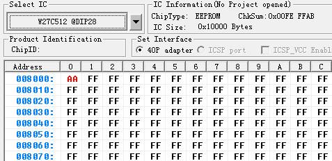
Сейчас вы спросите, зачем нужны оба? Я говорю, что один первый нужен для модифицированной прошивки, то есть именно с ним вы будете работать основную часть работы. Туда вы будете записывать таблицы зажигания, и топливные карты, так же и точки VTEC. Второй чип памяти нужен только в том случае, если вы хотите узнать какая прошивка сейчас стоит уже в блоке, то есть оригинальная прошивка. Чаще всего оригинальная прошивка уже списана кем-то другим и находится в репозитории PGMFI.org. Если это так, то статью про Даталог можете вообще не читать, ибо оригинальная прошивка есть на сайте, и вы можете перейти непосредственно к прошивке 29c256. Кстати оба чипа памяти программируется только параллельным программатором
27с256 или 29с256
27 или 29. Это тип перезаписи чипа микросхемы. Первая стирается ультрафиолетом, является, на мой взгляд, менее практичной в данных условиях. Да и установку с ультрафиолетом сейчас не найдешь. Если все таки вы взяли память EPROM 27C256 (как Winbond W27C256-45z) то данная микросхема является одноразовой. Вторая это 29. Стирается электрически, поддерживается максимальным количеством программаторов. Мой выбор и совет 29C256 — Тоесть всяческие M29C256, AT28C256 и прочее. Бытует мнение что если установить 27С512 или 29C512 то в 512кб памяти можно будет записать много прошивок.вы не сможете это реализовать. Потому что первая ножка в 256 отвечает за WE (запись разрешена), а в 512 отвечает за A15 Бит доступа адреса. То есть назначение ножек различное, НО 512 использовать можно, если программировать с адреса h008000.
Совет по чипу
Ввиду того что чип будет прошиваться несколько раз, и его придется вытаскивать советую установить его в разъем кроватку на 28 ног. Сначало впайяте кроватку на плату а потом установите микросхему. Для более удобного и безопасного извлечения используете кроватку с фиксатором, если же такой кроватки по микросхему нет то просто проденьте нить под микросхемой.
Как установить чип P28 (или подобного P08, P72, P06) OBD1
После того как соберете весь набор, за исключением последних 6 пунктов, то можете приступать к работе. Сначала растворителем тщательно обработайте поверхность платы P28 OBD1 от лака, протрите тампоном, смоченном в растворителе, участок, где будете ставить элементы.
Разогрейте хорошо паяльник, возьмите флюс или оплетку с флюсом, приложите оплетку к участку с запаянным местом и нагрейте паяльником. После удаления с обеих сторон, припой, возможно, останется. Возьмите канцелярскую скрепку, разогните её, и используйте ее вместе с паяльником для увеличения отверстий. Когда все посадочные места будут готовы, установите: 1 резистор, 2 Конденсатора, 2 кроватки. Я использовал отечественные элементы с большим запасом прочности и мощности, предварительно проверив их, конечно.
Место JN1 оставьте не тронутым, я установил туда 2 штыря (на подобии как делают на жестких дисках компьютера), если я не хочу пользоваться прошивкой, я просто использую перемычку. Если же мне нужна штатная прошивка, я просто отсоединяю перемычку. Делайте все аккуратно, не задевайте другие элементы, следите, чтобы припой не замкнул два соседних контакта. После пайки проверьте контакты мульти-тестером, очистите плату от флюса при помощи спирта или растворителя. Проверьте еще раз плату на наличие маленьких проводков, которые могут замкнуть контакты.